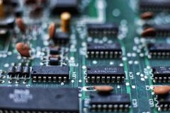
Semiconductor & Electronics Manufacturing Applications
Application Overview
How Our Products Support Your Industry
Key Applications and Solutions
Flow Measurement & Control
Accurate flow measurement and control are vital in semiconductor and electronics manufacturing to ensure process consistency, product quality, and operational efficiency. Precise management of liquid and gas flows is essential in various stages of production, from chemical vapor deposition to etching and cleaning processes. Implementing reliable flow measurement systems helps maintain optimal conditions, minimize waste, and prevent contamination, thereby enhancing overall yield and compliance with industry standards.
Applications of Flow Measurement & Control in Semiconductor and Electronics Manufacturing Applications
- Chemical Vapor Deposition (CVD): Precise control of gas flow rates is essential for uniform thin-film deposition, affecting the performance of semiconductor devices. Mass flow controllers are commonly used to regulate these gas flows accurately.
- Etching Processes: Accurate measurement of etchant flow ensures consistent material removal rates, critical for defining circuit patterns. Non-invasive flow meters can monitor these corrosive chemicals without direct contact, enhancing safety and reliability.
- Chemical Mechanical Planarization (CMP): Controlling the flow of slurry mixtures during CMP is crucial for achieving the desired surface planarity of wafers. Reliable flow meters help maintain the correct slurry composition and flow rate, impacting device performance.
- Ultrapure Water Delivery: Ultrapure water is used extensively for wafer rinsing and cleaning. Ensuring accurate flow measurement in these systems prevents contamination and maintains process integrity.
Key Purchasing Considerations
- Compatibility with Process Media: Ensure that the flow meter materials are compatible with the chemicals or gases being measured to prevent corrosion and contamination. For instance, non-invasive ultrasonic flow meters are suitable for aggressive chemicals.
- Measurement Accuracy and Range: Choose instruments that provide the required accuracy and can operate effectively within the expected flow rates of your processes.
- Cleanliness and Purity Requirements: Opt for flow meters designed to meet the stringent cleanliness standards of semiconductor manufacturing, such as those compatible with ultrapure water systems.
- Installation and Maintenance: Consider the ease of installation and maintenance. Non-invasive flow meters, for example, offer the advantage of being installed without process interruption and reduce the risk of leaks.
- Integration with Control Systems: Ensure that the chosen flow meters can integrate seamlessly with existing control and data acquisition systems, facilitating real-time monitoring and automation.
Level Measurement & Monitoring
Precise level measurement and monitoring play a critical role in semiconductor and electronics manufacturing, where maintaining accurate chemical, gas, and ultrapure water levels is essential for process consistency and contamination prevention. Reliable level instrumentation ensures efficient material usage, prevents costly overflows or shortages, and helps maintain compliance with stringent industry standards. By utilizing advanced technologies such as ultrasonic, radar, and capacitance level sensors, manufacturers can achieve accurate and non-intrusive monitoring of various liquids and gases used in production processes.
Applications of Level Measurement & Monitoring in Semiconductor and Electronics Manufacturing Applications
- Chemical Storage and Delivery Systems: Accurate level monitoring in bulk and day tanks ensures a consistent supply of process chemicals while preventing overfills and depletion that could disrupt manufacturing operations.
- Ultra-Pure Water (UPW) Systems: Semiconductor fabrication requires vast amounts of UPW for wafer cleaning and rinsing. Continuous level monitoring in UPW storage tanks and distribution systems helps maintain purity and prevent contamination.
- Slurry and Chemical Mechanical Planarization (CMP) Processes: CMP slurries used in wafer polishing must be carefully maintained at optimal levels to ensure uniform material removal and minimize defects.
- Wastewater and Effluent Management: Level measurement in waste collection and neutralization tanks helps manage the proper treatment and disposal of hazardous chemicals while ensuring compliance with environmental regulations.
- Vacuum and Gas Chambers: Monitoring gas levels in vacuum deposition and etching chambers is crucial for process stability, ensuring optimal pressure conditions and preventing material waste.
Key Purchasing Considerations
- Material Compatibility: Ensure the level sensor materials are resistant to highly corrosive chemicals such as acids, solvents, and etchants commonly used in semiconductor fabrication.
- Non-Contact vs. Contact Sensors: Non-contact technologies (e.g., radar or ultrasonic sensors) are preferred for applications involving aggressive chemicals or stringent cleanliness requirements. Contact sensors (e.g., capacitance or guided wave radar) may be suitable for specific applications where direct measurement is required.
- Precision and Accuracy Requirements: Given the critical nature of semiconductor processes, high-accuracy level measurement is essential to prevent process variations that can impact wafer quality.
- Environmental and Safety Compliance: The selected sensors should comply with industry standards for hazardous environments (e.g., explosion-proof ratings for certain chemical storage applications).
- Integration with Process Control Systems: Ensure compatibility with manufacturing execution systems (MES) or SCADA platforms for real-time monitoring, automated alarms, and predictive maintenance.
- Maintenance and Calibration Needs: Choose level sensors with minimal maintenance requirements and easy calibration procedures to reduce downtime and operational disruptions.
Pressure & Temperature Regulation
Precise pressure and temperature regulation are essential in semiconductor and electronics manufacturing, where even minor fluctuations can impact process stability, yield, and product quality. Advanced sensors, transmitters, and controllers help maintain optimal conditions in critical processes such as chemical vapor deposition (CVD), etching, lithography, and wafer cooling. Maintaining precise control over these parameters ensures uniformity, reduces defects, and enhances the reliability of semiconductor devices.
Applications of Pressure & Temperature Regulation in Semiconductor and Electronics Manufacturing Applications
- Chemical Vapor Deposition (CVD) and Plasma Etching: Pressure regulation is vital in maintaining the correct vacuum levels required for thin-film deposition and etching processes. Consistent temperature control ensures uniform film growth and material removal.
- Lithography and Photoresist Processing: Temperature stability is essential in lithography equipment to prevent distortions in photomask alignment and improve resolution. Pressure-controlled vacuum systems also ensure proper adhesion of photoresist layers.
- Wafer Cleaning and Drying: Proper pressure and temperature regulation in ultrapure water and gas-based drying systems prevent contamination and ensure complete particle removal.
- Gas Flow and Delivery Systems: Semiconductor fabrication uses various specialty gases for doping, oxidation, and etching. Accurate pressure regulation ensures consistent gas flow rates, preventing variations that could affect process outcomes.
- Thermal Processing and Annealing: High-temperature annealing processes are used to modify semiconductor material properties. Precision temperature control ensures uniform heating and cooling cycles, preventing stress-induced defects.
Key Purchasing Considerations
- Accuracy and Stability: Choose sensors and controllers with high precision to maintain stable pressure and temperature conditions, minimizing fluctuations that could affect process quality.
- Material Compatibility: Ensure components can withstand exposure to high temperatures, reactive gases, and corrosive chemicals used in semiconductor processes.
- Response Time and Sensitivity: Fast response times are crucial in maintaining real-time control in dynamic manufacturing environments, preventing overheating or pressure deviations.
- Integration with Control Systems: Sensors and regulators should be compatible with automated control platforms such as PLCs, SCADA, or MES for seamless process monitoring and optimization.
- Environmental and Safety Considerations: Instruments should meet cleanroom standards and safety certifications, including explosion-proof ratings for hazardous gas applications.
- Maintenance and Calibration Needs: Regular calibration is critical for maintaining measurement accuracy. Choosing sensors with self-diagnostic or predictive maintenance capabilities can reduce downtime.
Gas Detection & Environmental Monitoring
Maintaining a safe and controlled manufacturing environment is critical in semiconductor and electronics production, where hazardous gases, airborne contaminants, and strict cleanroom conditions must be carefully managed. Gas detection and environmental monitoring solutions help ensure worker safety, process integrity, and compliance with industry regulations. Advanced sensor technologies enable real-time detection of toxic and flammable gases, as well as continuous monitoring of air quality parameters, minimizing risks and preventing costly contamination events.
Applications of Gas Detection & Environmental Monitoring in Semiconductor and Electronics Manufacturing Applications
- Hazardous Gas Detection: Semiconductor fabrication utilizes various hazardous gases, such as arsine, phosphine, silane, and hydrogen chloride. Continuous monitoring helps detect leaks early, preventing exposure risks and ensuring facility safety.
- Cleanroom Air Quality Control: Particle contamination can lead to defects in semiconductor devices. Environmental monitoring systems track airborne particulate levels, ensuring compliance with ISO cleanroom standards.
- Vacuum System and Exhaust Monitoring: Monitoring gas composition in vacuum chambers and exhaust systems ensures that hazardous byproducts are properly contained and removed, maintaining process stability.
- Chemical Storage and Distribution: Real-time monitoring of gas levels in chemical storage areas helps prevent leaks, fire hazards, and accidental overexposure to toxic substances.
- Oxygen and Ventilation Monitoring: Proper ventilation and oxygen level monitoring are essential in confined spaces where inert gases, such as nitrogen, are used, reducing the risk of asphyxiation.
- Electrostatic Discharge (ESD) and Humidity Control: Semiconductor production requires strict humidity control to prevent electrostatic discharge, which can damage sensitive components. Environmental monitoring systems help regulate humidity levels to protect manufacturing processes.
Key Purchasing Considerations
- Sensor Sensitivity and Detection Range: Ensure the gas detection system is capable of identifying even trace amounts of hazardous gases with high sensitivity.
- Response Time and Alarm Capabilities: Fast-acting sensors with real-time alerts enable immediate response to potential gas leaks, reducing safety risks.
- Integration with Facility Management Systems: Gas detection systems should seamlessly integrate with existing building automation, fire suppression, and SCADA systems for centralized monitoring and emergency response.
- Compliance with Industry Standards: Instruments should meet semiconductor industry safety regulations such as SEMI S2, OSHA, and NFPA guidelines.
- Maintenance and Calibration Requirements: Select sensors with low maintenance requirements and automated calibration features to ensure long-term accuracy and reliability.
- Multi-Gas Detection Capabilities: Depending on the manufacturing processes, a system that detects multiple gases simultaneously may be more effective and cost-efficient than standalone sensors.
Industrial Automation & Data Integration
The semiconductor and electronics manufacturing industry relies heavily on industrial automation and data integration to enhance precision, efficiency, and scalability. As production processes become increasingly complex, seamless automation and real-time data analytics enable manufacturers to optimize workflows, reduce downtime, and maintain compliance with stringent industry standards. Integrating advanced sensors, IoT-enabled devices, and control systems ensures a high level of process control while enabling predictive maintenance and continuous monitoring.
Applications of Industrial Automation & Data Integration in Semiconductor and Electronics Manufacturing Applications
- Supervisory Control and Data Acquisition (SCADA) Systems: SCADA systems provide real-time monitoring and control of manufacturing processes, enabling operators to track critical parameters and respond quickly to deviations.
- Manufacturing Execution Systems (MES): MES platforms integrate process data, quality control, and production scheduling to improve efficiency and traceability throughout semiconductor fabrication.
- IoT-Enabled Process Monitoring: Smart sensors and IoT devices collect and transmit real-time process data, allowing for advanced analytics, remote monitoring, and predictive maintenance.
- Automated Material Handling Systems: Robotics and conveyor systems streamline wafer transport, reducing contamination risks and improving throughput in cleanroom environments.
- AI-Driven Defect Detection: Machine learning algorithms analyze process data to identify defects in wafers and circuits, improving product quality and reducing waste.
- Digital Twin Technology: Virtual replicas of manufacturing processes allow for simulation, optimization, and predictive analysis before implementing changes in real-world production.
Key Purchasing Considerations
- System Compatibility and Interoperability: Ensure that automation solutions integrate seamlessly with existing SCADA, MES, and enterprise resource planning (ERP) systems.
- Real-Time Data Processing and Analytics: Advanced data acquisition and processing capabilities enable immediate decision-making and process optimization.
- Scalability and Flexibility: Choose modular and scalable automation solutions that can adapt to future production expansions or technological advancements.
- Cybersecurity and Data Protection: As manufacturing processes become more interconnected, ensuring secure data transmission and system protection against cyber threats is crucial.
- Regulatory Compliance: Automation systems should align with semiconductor industry standards, such as SEMI E10 (Equipment Performance Standards) and ISO 9001 for quality management.
- Maintenance and Lifecycle Costs: Consider long-term operational costs, including system updates, software licensing, and hardware maintenance, to maximize return on investment.
Industry Standards & Regulatory Compliance
Key Regulatory & Industry Standards for Semiconductor Manufacturing
- SEMI F47: Addresses power quality requirements for equipment, ensuring continuity during voltage sags.
- SEMI F57: Specifies purity requirements for ultra-high-purity (UHP) polymer components in UPW systems.
- SEMI S2 & S8: Establish safety guidelines for equipment design, including emergency shutoffs, gas leak detection, and ergonomic considerations.
- SEMI E49.4: Covers gas distribution and flow control equipment for high-purity and hazardous gases.
- Regulates emissions from point sources such as thermal oxidizers, scrubbers, and abatement systems.
- Semiconductor processes using perfluorinated compounds (PFCs), HF, HCl, and VOCs must monitor and report emissions using real-time gas analyzers and flow monitoring systems.
- Requires control and reporting of greenhouse gases (GHGs) under the Greenhouse Gas Reporting Program (GHGRP).
- Fabrication facilities must treat and monitor wastewater discharges for fluorides, heavy metals (e.g., copper, lead), acids, and solvents.
- Facilities typically require pH sensors, conductivity analyzers, TOC monitors, and flow meters to comply with NPDES permits or local pretreatment program limits.
OSHA Process Safety Management (PSM) – 29 CFR 1910.119:
- Applies to facilities using toxic, flammable, or reactive chemicals such as silane, arsine, and hydrogen chloride.
- Requires integration of automated safety shutdown systems, gas leak detectors, pressure monitors, and temperature alarms to minimize operational risk.
- Emphasizes routine sensor calibration, alarm testing, and control loop verification for compliance and audit readiness.
Cleanroom & Product Quality Compliance (ISO & Facility-Specific Standards)
- ISO 14644 – Cleanroom Standards: Defines air cleanliness classes and monitoring requirements for particle count, pressure, temperature, and humidity. Requires real-time cleanroom monitoring systems with data logging and alert capabilities.
- ISO 9001 & ISO 14001: Used to establish quality management and environmental management systems respectively. Requires traceability of process control data, incident logs, and continuous improvement initiatives.
- ESD & Electromagnetic Compliance: Instrumentation must be compatible with anti-static and EMI-sensitive environments, particularly in wafer-level packaging and assembly operations.
Benefits of Working With Clipper Controls